Titanym
Building the semiconductor stack silicon cannot reach.
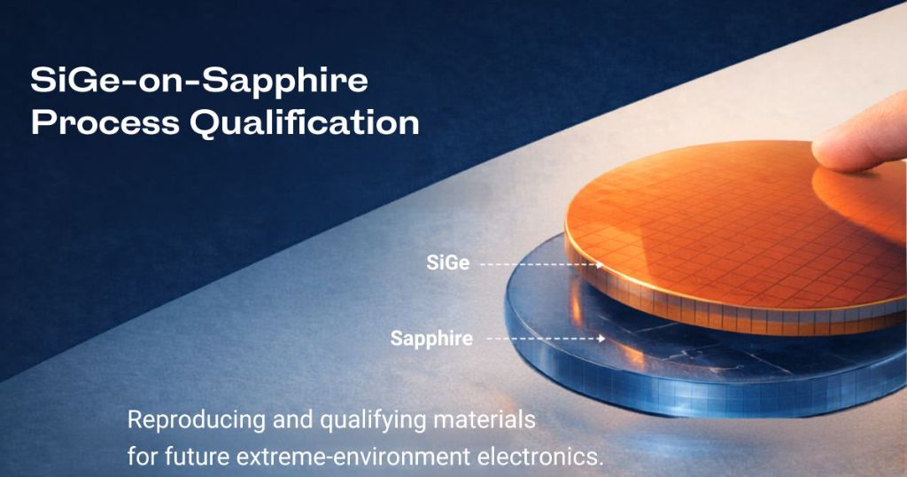
Titanym is a specialized semiconductor manufacturing program developing a process platform around single-crystal silicon-germanium on sapphire. Built for space, defense, RF, and advanced device markets where standard process flows fall short.
Phase 1 is underway: process reproduction and materials qualification, before device development begins.
Silicon is not the ceiling. It is the starting point.
Single-crystal silicon-germanium grown on sapphire substrates offers a combination of material performance, process economics, and integration potential that silicon alone cannot match. Particularly for device categories where substrate behavior, thermal management, defect control, and heterogeneous integration drive value.
Titanym is not competing with TSMC or Intel on leading-edge logic. The goal is different: own a narrow, high-consequence manufacturing stack that enables device classes standard foundries are not designed to serve.
Four times the carrier mobility
Single-crystal SiGe delivers substantially higher electron and hole mobility compared to standard silicon, enabling faster, lower-power device performance.
Radically simplified manufacturing
A mask-based deposition process reduces CMOS fabrication from 19 conventional steps to 8, eliminating photoresist, UV exposure, and most selective etching steps.
Low-temperature growth
SiGe-on-sapphire growth at 450 to 500C versus the conventional 850 to 900C range. Less thermal load, faster cycle times, higher throughput potential.
A narrow process advantage in a high-consequence market.
Standard silicon process flows are optimized for volume and cost at scale. They are not designed for the material requirements of extreme-environment electronics, specialized RF devices, or heterogeneous integration across substrates.
Titanym's foundation is a set of interlocking manufacturing capabilities, each addressing a specific technical bottleneck in specialty semiconductor production. The sapphire substrate enables SiGe electronics on one side and III-nitride device structures on the other, opening paths toward integrated compute and photonics on a single wafer.
The manufacturing stack.
Titanym's foundation is a set of interlocking manufacturing capabilities, each addressing a specific commercial and technical bottleneck in specialty semiconductor production.
Low-Temperature SiGe Epitaxy
A fabrication method that reduces SiGe-on-sapphire growth temperature from the conventional range down to 450 to 500C, eliminating thermal soak requirements and reducing production time from over four hours to under one hour without sacrificing crystal quality.
Single-Crystal Manufacturing Suite
A broader suite of process methods including Molten Target Sputtering, Thermally Absorptive Coating for faster heating, graded-index layer growth, and methods for thicker, denser, more crack-resistant crystal films.
Defect Control and Heteroepitaxy
Crystal orientation alignment with the sapphire substrate lattice minimizes misfit dislocation defects. Twin defect volume reduced to well under one percent. X-ray diffraction methods map defect structure across the full wafer.
Simplified CMOS Manufacturing
A mask-based deposition process that eliminates photoresist, UV exposure, and selective etching steps. Achieves the same result in 8 steps versus the conventional 19-step process, reducing cost, cycle time, and chemical waste.
Qualification first. Device development later.
Phase 1 is strictly scoped. The objective is to determine whether the SiGe-on-sapphire process can produce repeatable, high-quality semiconductor material. No device claims are made until this materials determination is complete.
Process Reproduction
Reproducing low-temperature SiGe growth at 450 to 500C from reported process parameters in a controlled nanofabrication environment.
Crystal Structure and Lattice Alignment
Measure crystal quality, orientation, and structural integrity of deposited SiGe layers including single-crystal confirmation and SiGe orientation alignment.
Defect Density and Twin Formation
Evaluate defect density and twin formation using X-ray diffraction: dislocations, twin defects, and contamination mapping across the deposited layer.
Wafer Stress and Surface Morphology
Analyze wafer stress through curvature analysis and thermal load performance testing, combined with AFM and microscopy for surface roughness and defect counts.
Repeatability Across Runs
Test reproducibility across multiple growth runs with statistical analysis and clear pass criteria applied to the full dataset.
Materials Qualification Report. A formal qualification report documenting all measurement data, process parameters, and material characterization findings, with a binary determination on readiness for Phase 2 device development.
The Qualification Path
Phase 1 follows a defined evaluation sequence. Each step informs the next.
Reproduce Growth Conditions
Controlled deposition at target low-temperature parameters in a university nanofabrication environment.
Characterize Crystal Quality
XRD analysis, single crystal confirmation, SiGe orientation alignment, and defect density mapping.
Evaluate Repeatability
Multi-run statistical analysis with documented variance across surface condition, wafer stress, and defect uniformity.
Produce Qualification Report
Full measurement record documenting all process parameters, material characterization findings, and readiness determination.
Issue Materials Determination
A formal readiness evaluation on whether the material system is prepared for subsequent device development work.
SiGe-on-Sapphire Wafer Qualification
Five measurement categories define the materials qualification standard for Phase 1.
Crystal Quality
- Single crystal confirmation
- SiGe orientation alignment
Defect Structure
- X-ray diffraction for dislocations
- Twin defects and contamination mapping
Wafer Stress
- Curvature analysis for internal stress
- Thermal load performance
Surface Condition
- AFM and microscopy analysis
- Defect counts and surface roughness
Repeatability
- Statistical analysis across multiple wafer runs
- Documented variance and pass criteria per category
Four phases. One platform.
Titanym builds toward a specialized semiconductor manufacturing platform through a disciplined, phase-controlled progression from process validation through proprietary product development.
Process Qualification — Active
Reproduce the low-temperature SiGe-on-sapphire growth process in a controlled nanofabrication environment. Characterize crystal quality, defect structure, surface morphology, and repeatability. Output is a materials qualification report.
Engineering Services
Paid feasibility projects, wafer development engagements, custom device prototyping, and process transfer work with government and commercial customers. This phase converts process knowledge into contracted revenue.
Device Manufacturing
Low-volume specialty manufacturing, custom runs for high-value customers, and recurring process-service contracts in space, defense, and RF verticals.
Proprietary Products
Selective launch of proprietary device lines in target verticals where Titanym's process advantage and customer knowledge create defensible product positions with recurring margin.
A substrate that does more than anchor the device.
Sapphire is electrically insulating, thermally stable, and optically transparent. It enables SiGe electronics on one face and III-nitride device structures on the other, a combination no standard substrate can match.
Single-crystal SiGe grown on sapphire maintains structural coherence with the substrate lattice, minimizing misfit dislocations and producing a semiconductor layer with well-controlled electronic properties. This combination is what Titanym is built to manufacture at process scale.
Electrical Isolation
Sapphire's insulating properties eliminate substrate leakage paths, reducing parasitic coupling and enabling cleaner RF device behavior compared to bulk silicon substrates.
Radiation Hardness
SiGe-on-sapphire demonstrates strong resistance to radiation-induced charge buildup, making it well-suited for satellite systems, deep-space instruments, and mission-critical payloads.
Optical Transparency
Sapphire transmits across visible and near-infrared wavelengths, enabling double-sided architectures that combine electronic and photonic device structures on a single substrate.
Monolithic Integration Potential
The sapphire substrate enables SiGe electronics on one side and III-nitride device structures on the other, opening paths toward integrated compute and photonics on a single wafer.
Where the process advantage matters most.
Titanym's commercial focus is on markets where reliability, differentiated process performance, and specialized integration matter more than commodity volume.
Space and Radiation-Hardened Electronics
SiGe on sapphire demonstrates strong radiation hardness, making it well-suited for satellite systems, deep-space instruments, and mission-critical payloads that cannot tolerate single-event upsets.
RF and High-Frequency Communications
SiGe heterojunction bipolar transistors already power RF front-ends in 5G base stations, satellite communications, and radar. The Titanym process opens a pathway to specialized RF device manufacturing.
Aerospace and Defense Sensing
Harsh-environment sensing applications benefit directly from rugged substrate performance, extended operational temperature range, and process-controlled reliability.
Optoelectronics and Display
Double-sided sapphire structures enable LED devices on one face and solar or electronic structures on the other, creating a platform for integrated, self-powered display architectures.
Energy Conversion Devices
SiGe's Type II band-gap alignment enables solar cell architectures with projected efficiencies of 30 to 40 percent, along with thermoelectric generator applications for waste heat recovery.
Co-Development Manufacturing
Government agencies, aerospace primes, and specialty hardware companies seeking non-standard semiconductor process support represent a direct co-development and process services opportunity.
Execution Environment
Titanym operates as a structured program under Umanah Systems Group with defined scope, phase-controlled progression, and institutional manufacturing access. Phase 1 runs within a university nanofabrication facility capable of controlled deposition, materials characterization, and full metrology.
Program Structure
Titanym operates as a program under Umanah Systems Group with defined scope, deliverables, and phase gates. A structured technical program with a disciplined commercialization pathway.
Nanofabrication Environment
Phase 1 runs within a university nanofabrication facility with access to controlled deposition, materials characterization equipment, and process expertise. Institutional access rather than new facility construction.
Current Focus
Phase 1 is strictly process reproduction and materials evaluation. Device development is not in scope until the materials determination is issued. This discipline is intentional.
Program Status
Phase 1 is active. The program is carrying out process reproduction, materials qualification, and readiness evaluation. Seeking technical collaborators and institutional partners for controlled process work.
Program Contact
For technical collaboration, institutional partnership, or program discussion inquiries.